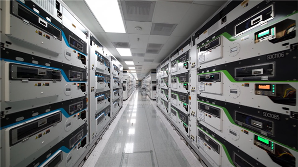
快科技4月30日消息,在今天的晶圆代工业务大会上,Intel公开了最新的工艺制程路线图,并分享了代工业务最新进展。
Intel披露的数据显示,在2021年提出“四年五个工艺节点”计划至2024年这四年间,Intel在全球的资本支出达到了900亿美元。
其中约180亿美元投向了技术研发,370亿美元投向了晶圆厂设备支出。
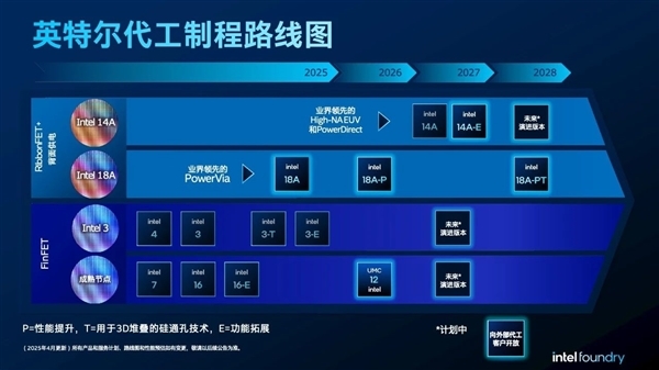
Intel表示,18A制程节点已进入风险试产阶段,预计将在今年实现量产,而18A之后的下一代14A工艺制程,则将在2027年前后进入风险生产阶段。
14A预计将带来15%-20%的能效提升,以及芯片密度增加1.3倍,同时已有几个客户计划流片14A测试芯片。
相对于Intel 18A采用的PowerVia背面供电技术,Intel 14A将采用PowerDirect直接触点供电技术。
Intel还公布了18A工艺的两个变体——18A-P和18A-PT,其中Intel 18A-P将带来更卓越的性能,早期试验晶圆目前已经开始生产,并且与Intel 18A的设计规则兼容。
Intel 18A-PT是在Intel 18A-P的性能和能效进步基础上推出的另一种Intel 18A演进版本,可通过Foveros Direct 3D先进封装技术与顶层芯片连接,混合键合互连间距小于5微米。
Foveros Direct 3D目前台积电已在生产中使用,最为消费者所熟知的就是AMD的3D V-Cache产品。
成熟节点方面,Intel代工流片的首批基于16纳米制程的产品已经进入晶圆厂生产,还正在与主要客户洽谈与UMC合作开发的12纳米节点及其演进版本。