英特尔代工:Intel 18A制程节点已进入风险试产阶段,将于今年量产

新浪科技
Yesterday

  新浪科技讯 4月30日上午消息,2025英特尔代工大会(Intel Foundry Direct Connect)上,英特尔分享了多代核心制程和先进封装技术的最新进展,并宣布了新的生态系统项目和合作关系。

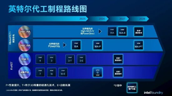
  据悉,在制程技术方面,英特尔代工已与主要客户就Intel 14A 制程工艺展开合作,发送了Intel 14A PDK(制程工艺设计工具包)的早期版本。这些客户已经表示有意基于该节点制造测试芯片。相对于Intel 18A所采用的PowerVia背面供电技术,Intel 14A将采用PowerDirect直接触点供电技术。

  同时,Intel 18A制程节点已进入风险试产阶段(in risk production),并将于今年内实现正式量产(volume manufacturing)。英特尔代工的生态系统合作伙伴为Intel 18A提供了EDA支持,参考流程和知识产权许可,让客户可以基于该节点开始产品设计。

  Intel 18A制程节点的演进版本Intel 18A-P,将为更大范围的代工客户带来更卓越的性能。Intel 18A-P的早期试验晶圆(early wafers)目前已经开始生产。由于Intel 18A-P与Intel 18A的设计规则兼容,IP和EDA合作伙伴已经开始为该演进节点提供相应的支持。

  Intel 18A-PT是在Intel 18A-P的性能和能效进步基础上推出的另一种Intel 18A演进版本。Intel 18A-PT可通过Foveros Direct 3D先进封装技术与顶层芯片连接,混合键合互连间距小于5微米。

  此外,英特尔代工流片的首批基于16纳米制程的产品已经进入晶圆厂生产。英特尔代工也正在与主要客户洽谈与UMC合作开发的12纳米节点及其演进版本。

  英特尔首席执行官陈立武表示:“英特尔致力于打造世界一流的代工厂,以满足日益增长的对前沿制程技术、先进封装和制造的需求。我们的首要任务是倾听客户的声音,提供有助于其成功的解决方案,以赢得客户的信任。”(文猛)

海量资讯、精准解读,尽在新浪财经APP

责任编辑:郝欣煜

Disclaimer: Investing carries risk. This is not financial advice. The above content should not be regarded as an offer, recommendation, or solicitation on acquiring or disposing of any financial products, any associated discussions, comments, or posts by author or other users should not be considered as such either. It is solely for general information purpose only, which does not consider your own investment objectives, financial situations or needs. TTM assumes no responsibility or warranty for the accuracy and completeness of the information, investors should do their own research and may seek professional advice before investing.

Most Discussed

  1. 1


  2. 2


  3. 3


  4. 4


  5. 5


  6. 6


  7. 7


  8. 8


  9. 9


  10. 10