炒股就看金麒麟分析师研报,权威,专业,及时,全面,助您挖掘潜力主题机会!
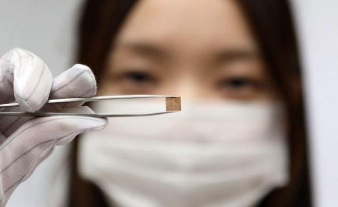
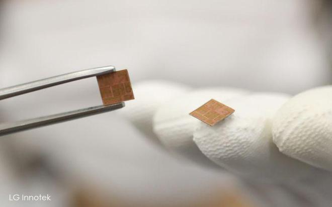
IT之家 6 月 27 日消息,韩国先驱报于 6 月 25 日发布博文,报道称 LG Innotek 宣布开发出全球首个用于高端半导体基板的高价值铜柱(Cu-Post)技术,在保持性能的前提下,让智能手机基板尺寸最高可减少 20%,为更轻薄、高性能手机的发展迈出重要一步。
随着全球智能手机制造商竞相提升设备性能并最小化设备厚度,对先进且紧凑的半导体基板技术的需求急剧增长。
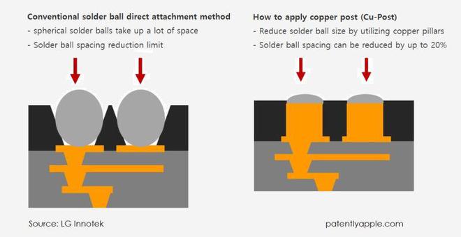
LG Innotek 预测这一趋势,于 2021 年开始研发下一代 Cu-Post 技术。与传统的直接使用焊球连接基板和主板的方法不同,Cu-Post 技术利用铜柱来减小焊球的间距和大小。
这项技术不仅减少了基板尺寸,还支持更密集的电路布局,从而在不影响性能的前提下提高集成度。LG Innotek 表示,应用 Cu-Post 技术后,保持相同的性能水平的情况下,半导体基板的尺寸最高可减小 20%。
这项技术还显著改善了设备的散热性能。铜的导热性是传统焊球的七倍以上,能够更快地从半导体封装中散热。
该公司已经制定了雄心勃勃的计划,到 2030 年将半导体组件业务 —— 以高端基板和汽车应用处理器模块为核心 —— 发展成为年销售额达 3 万亿韩元(IT之家注:现汇率约合 158.55 亿元人民币)的板块。
Disclaimer: Investing carries risk. This is not financial advice. The above content should not be regarded as an offer, recommendation, or solicitation on acquiring or disposing of any financial products, any associated discussions, comments, or posts by author or other users should not be considered as such either. It is solely for general information purpose only, which does not consider your own investment objectives, financial situations or needs. TTM assumes no responsibility or warranty for the accuracy and completeness of the information, investors should do their own research and may seek professional advice before investing.