台积电准备将CoWoS“面板化”,计划切换到CoPoS封装技术

市场资讯
Aug 16, 2025

  炒股就看金麒麟分析师研报,权威,专业,及时,全面,助您挖掘潜力主题机会!

(来源:超能网)

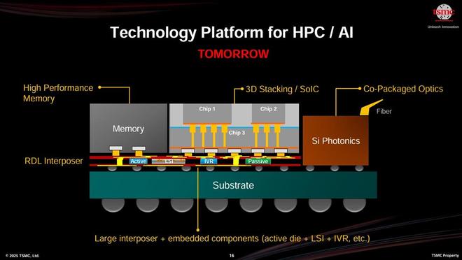
近年来,台积电(TSMC)除了积极投资先进制程节点,以保证竞争优势外,还逐步加大了在封装技术方面的投入力度,以满足新一代人工智能(AI)和高性能计算(HPC)芯片的需求。其中准备了新一代CoPoS(Chip-on-Panel-on-Substrate)封装技术,可以将基板扩展到310 × 310 mm甚至更大尺寸。

据DigiTimes报道,台积电正在准备改变先进封装战略,将CoWoS“面板化”,与扇出型面板级封装(FOPLP)技术整合,过渡到CoPoS封装技术。未来将采用方形基板,取代过去的圆型基板,这么做可以有效提升产能。

台积电计划最早于2026年建立首条oPoS封装生产线,进行试点生产,负责的工厂是中国台湾嘉义AP7的P4和P5,最快2028年末至2029年上半年量产,预计未来CoPoS将取代CoWoS-L。台积电已经大致敲定了首批设备的供应厂商,确立相关规格与订单量。

与FOPLP一样,CoPoS也采用大型面板基板进行封装,不过两者存在一些差异。FOPLP是一种不需要中介层的封装方法,芯片直接重新分布在面板基板上,并通过重分布层(RDL)互连。这种方法具有成本低、I/O密度高、外形尺寸灵活等优势,适用于边缘AI、移动设备和集成密度适中的中端ASIC等应用。CoPoS则引入了中介层,从而有着更高的信号完整性和稳定的功率传输,对于集成GPU和HBM芯片的高端产品来说效果更好。同时中介层材料正从传统的硅变为玻璃,将提供更高的成本效益和热稳定性。

海量资讯、精准解读,尽在新浪财经APP

Disclaimer: Investing carries risk. This is not financial advice. The above content should not be regarded as an offer, recommendation, or solicitation on acquiring or disposing of any financial products, any associated discussions, comments, or posts by author or other users should not be considered as such either. It is solely for general information purpose only, which does not consider your own investment objectives, financial situations or needs. TTM assumes no responsibility or warranty for the accuracy and completeness of the information, investors should do their own research and may seek professional advice before investing.

Most Discussed

  1. 1


  2. 2


  3. 3


  4. 4


  5. 5


  6. 6


  7. 7


  8. 8


  9. 9


  10. 10