大日本印刷(DNP)开发出了能以十分之一的耗电量生产先进半导体的技术。将面向佳能生产的新方式制造装置,于2027年量产可支持新一代1.4纳米(1纳米为十亿分之一米)产品的核心构件。人工智能(AI)半导体的制造成本有大幅降低的可能性。
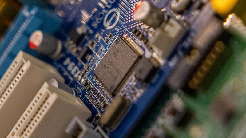
目前,要量产最先进的半导体,需要使用全球只有荷兰阿斯麦控股(ASML Holdings)生产的极紫外(EUV)光刻机。在晶圆(基板)上绘制电路的“光刻工序”占半导体总制造成本的3至5成。电路越精细,光刻次数就越多,耗电量也随之增加。一台EUV光刻机的价格为300亿日元左右,给半导体厂商带来沉重的投资负担。
而佳能的“纳米压印(Nanoimprint )”制造装置采用类似盖印章的方式在晶圆上制作电路。DNP开发出了相当于精细印章的电路原版“模板(template)” ,最高可用于1.4纳米制程。此前该技术无法支持2纳米等先进半导体的制造。
......
阅读更多内容请点击下方“阅读原文”
(本文由日经中文网提供)
Disclaimer: Investing carries risk. This is not financial advice. The above content should not be regarded as an offer, recommendation, or solicitation on acquiring or disposing of any financial products, any associated discussions, comments, or posts by author or other users should not be considered as such either. It is solely for general information purpose only, which does not consider your own investment objectives, financial situations or needs. TTM assumes no responsibility or warranty for the accuracy and completeness of the information, investors should do their own research and may seek professional advice before investing.