台积电更新SoIC 3D芯片路线图:2029年互连间距缩至4.5μm

IT之家
Yesterday

台积电更新SoIC 3D芯片封装堆叠技术路线图:2029年互连间距缩至4.5μm

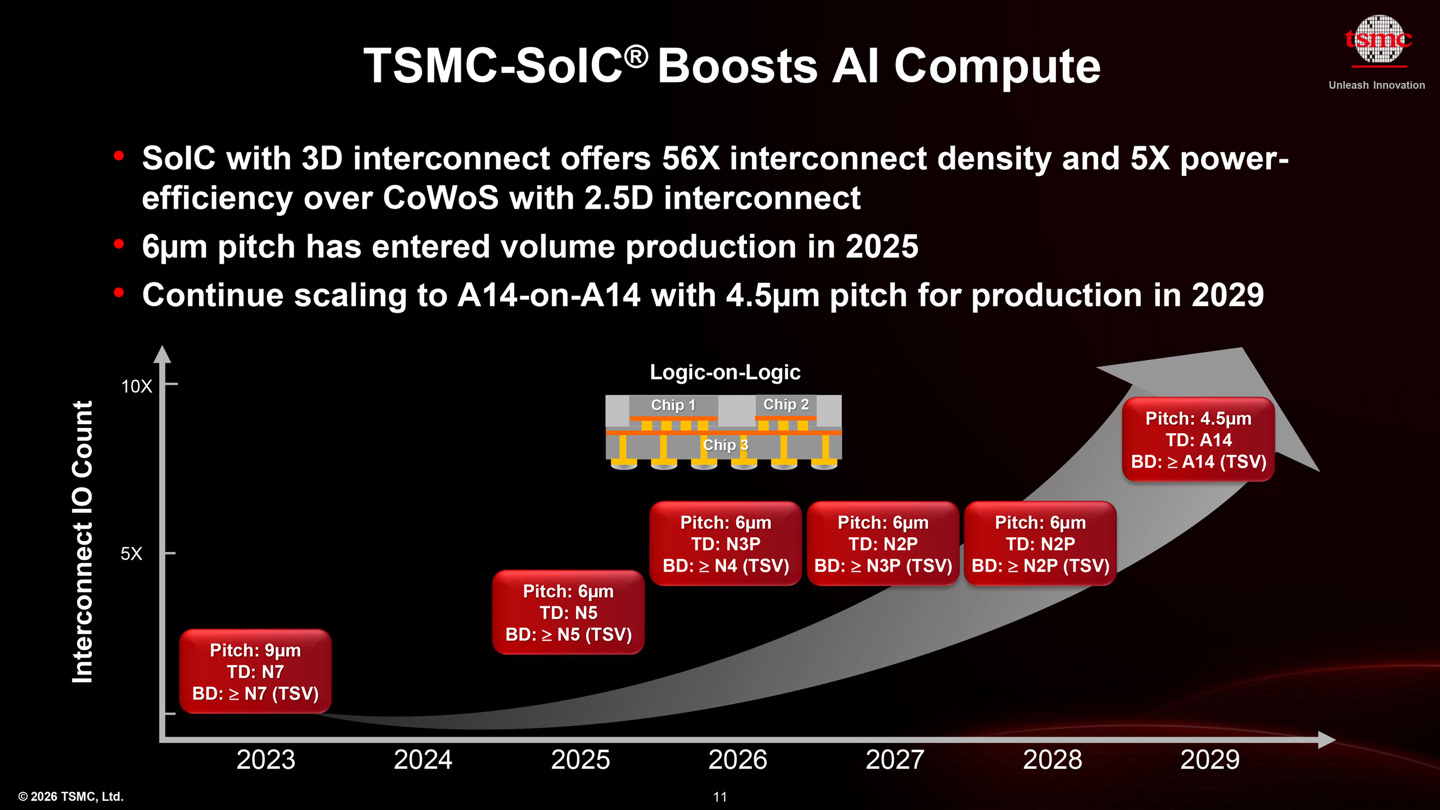
IT之家 4 月 30 日消息,在北美技术研讨会上,台积电更新公布 SoIC 3D 堆叠技术路线图,明确了未来几年的技术演进方向。台积电计划缩小现有的 6μm 互连间距,目标到 2029 年缩小至 4.5μm。

IT之家注:SoIC 全称 System on Integrated Chips,是台积电开发的 3D IC 封装技术,通过垂直堆叠多个芯片实现高性能、高密度的集成。

相比传统封装,SoIC 利用混合键合技术实现芯片间的直接互连,大幅缩短信号路径,降低功耗与延迟,适用于高性能计算与 AI 芯片。

在技术路径上,SoIC 主要分为 Face-to-Back(F2B,背对背)和 Face-to-Face(F2F,面对面)两种堆叠方式。F2B 堆叠受限于物理结构,信号必须穿过底部的硅通孔(TSV)和多层金属,不仅增加延迟和功耗,还限制了互连密度。

数据显示,F2B 设计的信号密度仅为 1500 个 / mm²。相比之下,F2F 堆叠通过混合铜键合技术直接连接两块芯片的金属层,无需使用 TSV,信号密度大幅提升至 14000 个 / mm²,让芯片间的通信性能接近片内互连水平。

从纯粹的互连间距来看,台积电在 2023 年实现了相当精细的 9µm 间距,足以支持 AMD Instinct MI300 系列等产品,但第一代 SoIC 仅支持 F2B 设计。台积电在 2025 年把互连间距缩短到 6μm,并预估到 2029 年间距将缩小至 4.5µm。

以上图源:台积电

富士通的 Monaka 处理器是该技术的首个重量级应用。这款面向数据中心的 CPU 拥有 144 个 Armv9 核心,其计算模块采用台积电 N2 工艺制造,并通过 F2F 方式堆叠在 N5 工艺的 SRAM 芯片之上。

Disclaimer: Investing carries risk. This is not financial advice. The above content should not be regarded as an offer, recommendation, or solicitation on acquiring or disposing of any financial products, any associated discussions, comments, or posts by author or other users should not be considered as such either. It is solely for general information purpose only, which does not consider your own investment objectives, financial situations or needs. TTM assumes no responsibility or warranty for the accuracy and completeness of the information, investors should do their own research and may seek professional advice before investing.

Most Discussed

  1. 1


  2. 2


  3. 3


  4. 4


  5. 5


  6. 6


  7. 7


  8. 8


  9. 9


  10. 10