IT之家 6 月 27 日消息,据科技媒体 Wccftech 昨天报道,亿万富翁埃隆 · 马斯克认为,IBM 前天公布的“0.7 纳米芯片”命名具有误导性质,并不能反映晶体管的真实尺寸。
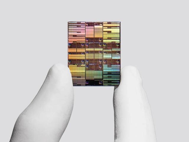
马斯克认为,未来芯片制程节点应当根据最小特征尺寸对应的原子数量命名,而不是沿用现有命名方式。
IBM 表示,公司的 0.7 纳米工艺是 Nanosheet(IT之家注:纳米片)基础上的进一步升级,并采用全新 Nanostack(纳米堆叠)技术。该公司宣称纳米堆叠技术可将晶体管垂直堆叠,提高芯片的晶体管密度,晶圆键合(Wafer Bonding)也是 0.7 纳米工艺的重要组成部分。
至于命名方式,IBM 解释道:
与近年来所有晶体管尺寸的命名方式一样,“7 埃(7Å)”指的是这一代采用特定制造工艺生产的芯片。
“7 埃”并不是指以前芯片中接触金属导线的实际宽度,那个年代的芯片集成密度远低于今天。
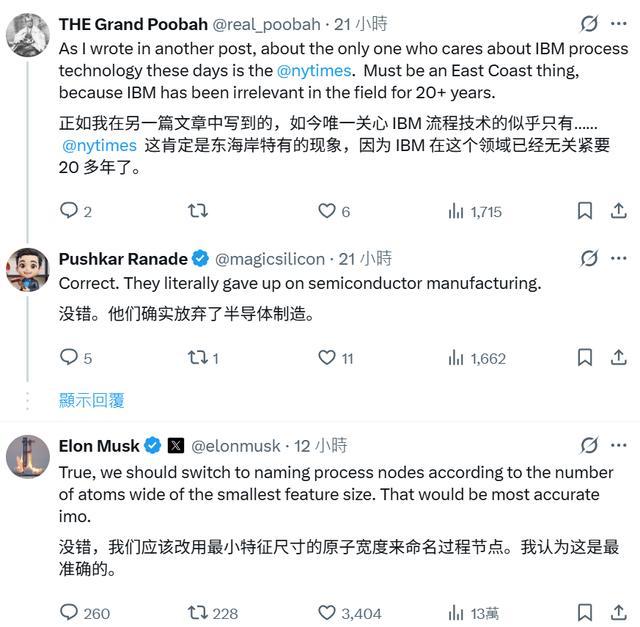
而马斯克则是在 X 平台上关注了一篇帖子,该帖文指出:“IBM 芯片实际印刷尺寸小于 1 纳米的特征数量为零。这种命名方式完全没有道理,而且极具误导性”。
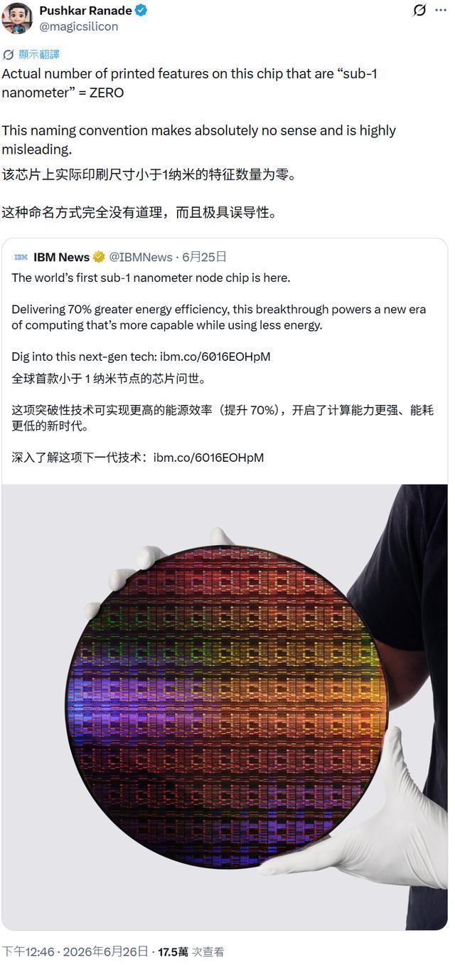
马斯克表达赞同后说道:“我们应该按照最小特征尺寸宽度对应的原子数量来命名制程节点。依我看,那才是最准确的命名方式”。
Disclaimer: Investing carries risk. This is not financial advice. The above content should not be regarded as an offer, recommendation, or solicitation on acquiring or disposing of any financial products, any associated discussions, comments, or posts by author or other users should not be considered as such either. It is solely for general information purpose only, which does not consider your own investment objectives, financial situations or needs. TTM assumes no responsibility or warranty for the accuracy and completeness of the information, investors should do their own research and may seek professional advice before investing.