英伟达公开Rubin GPU细节:3360亿晶体管,智能体AI性能提升10倍

IT之家
Jul 22

IT之家 7 月 22 日消息,英伟达今天(7 月 22 日)发布博文,公开 Rubin GPU 架构细节。该 GPU 基于台积电 3nm 工艺,集成 3360 亿个晶体管,在智能体 AI 性能方面,比 Blackwell 提升 10 倍。

架构方面,英伟达表示 Rubin GPU 采用台积电 3nm(N3P)工艺制造,由两块光罩极限尺寸 Die 实现高密度和高效率特性,这 2 个 Die 通过 NVIDIA 高带宽接口(NV-HBI)连接成统一封装,总计集成 3360 亿晶体管,较 Blackwell GB300 芯片增加 62%。
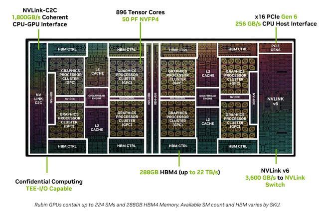
每个 Rubin GPU 内部包括 8 个 GPC(图形处理集群),总计 224 个 SM(流式多处理器)和 896 个 Tensor Cores。根据方框图,存在两种类型的 GPC:一种包含 30 个 SM,另一种包含 26 个 SM。

每个 Die 上配有 4 个 GPC,它们连接着两组大型去中心化 L2 缓存、一个 Gigathread Engine、四个 HBM 通道(每个芯片 4096 位)和一个 NVLink 接口。

NVLink 6 提供 3600 GB/s 的 GPU 间互联带宽,NVLink-C2C 接口提供 1800 GB/s 的 CPU 至 GPU 通信带宽,PCIe Gen6 x16 通道则提供 256 GB/s 的主机连接带宽。

在性能指标方面,NVIDIA 官方数据显示,针对智能体 AI 工作负载,Rubin 的单位能耗吞吐量达到 Blackwell 的 10 倍。
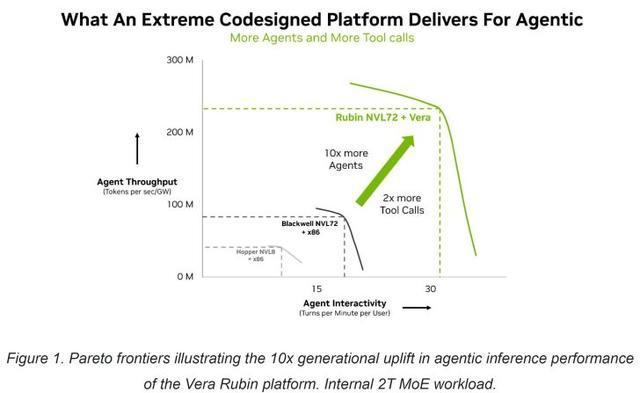
该提升源自三项主要架构变更:增强型张量核心(Tensor Cores)支持扩展精度、全新 HBM4 内存子系统以及第三代 Transformer 引擎。

内存系统方面,Rubin 搭载 8 个 12-Hi 堆栈的 HBM4 内存,总容量 288 GB,单堆栈容量 36 GB,峰值带宽达 22 TB/s,较 Blackwell 的 8 TB/s 提升了 1.8 倍。
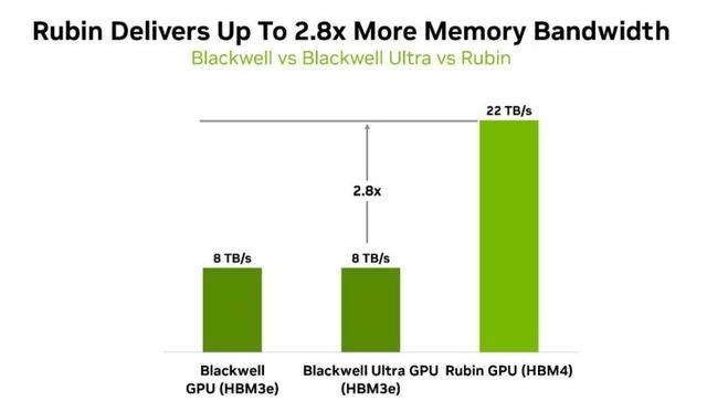
该内存方案支持更大上下文窗口、更高并发量,并在逐令牌生成阶段确保模型权重与 KV 状态的高速移动。
Disclaimer: Investing carries risk. This is not financial advice. The above content should not be regarded as an offer, recommendation, or solicitation on acquiring or disposing of any financial products, any associated discussions, comments, or posts by author or other users should not be considered as such either. It is solely for general information purpose only, which does not consider your own investment objectives, financial situations or needs. TTM assumes no responsibility or warranty for the accuracy and completeness of the information, investors should do their own research and may seek professional advice before investing.

Most Discussed

  1. 1


  2. 2


  3. 3


  4. 4


  5. 5


  6. 6


  7. 7


  8. 8


  9. 9


  10. 10