快科技7月28日消息,据摩根士丹利报告,谷歌正在设计一款名为Frozen V2的新一代TPU芯片,目标是将SRAM直接集成到硅片上,从而摆脱对台积电CoWoS封装技术的依赖。
SRAM是目前AI芯片中速度最快的缓存,负责存储AI模型运行时频繁调用的数据,传统做法是把SRAM做成独立芯片,再通过CoWoS封装技术与计算单元连接在一起,但CoWoS封装工艺复杂、成本高,而且封装环节会增加数据传输的延迟。
Frozen V2的思路是把SRAM直接做在计算单元的硅片上,省去封装环节。
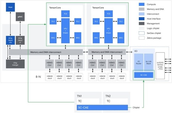
这样一来,数据不需要在芯片之间传输,速度更快,延迟更低,谷歌希望通过这种方式为Gemini模型量身定制芯片,专门优化AI推理性能。
不过这种方式也有代价,每次AI模型有重大升级时,都需要重新设计芯片,芯片制造商也要为每一轮生产调整设备。
AI芯片制造商Taalas今年早些时候也采用了类似方法,将神经网络权重直接集成到硅片上。
摩根士丹利预计,Frozen V2可在2027年进入早期生产,2028年量产,合作伙伴方面,Marvell可能是候选之一,但目前尚未确认。

Disclaimer: Investing carries risk. This is not financial advice. The above content should not be regarded as an offer, recommendation, or solicitation on acquiring or disposing of any financial products, any associated discussions, comments, or posts by author or other users should not be considered as such either. It is solely for general information purpose only, which does not consider your own investment objectives, financial situations or needs. TTM assumes no responsibility or warranty for the accuracy and completeness of the information, investors should do their own research and may seek professional advice before investing.