新型碳化硅SiC晶体管问世,可在600℃高温下工作

IT之家
5 hours ago

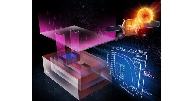
IT之家 8 月 25 日消息,科技媒体 Tom's Hardware 昨日(8 月 24 日)发布博文,报道称京都大学研究团队研发出新型碳化硅(SiC)晶体管,采用标准离子注入工艺制造,可在 600℃(873 K)下工作。

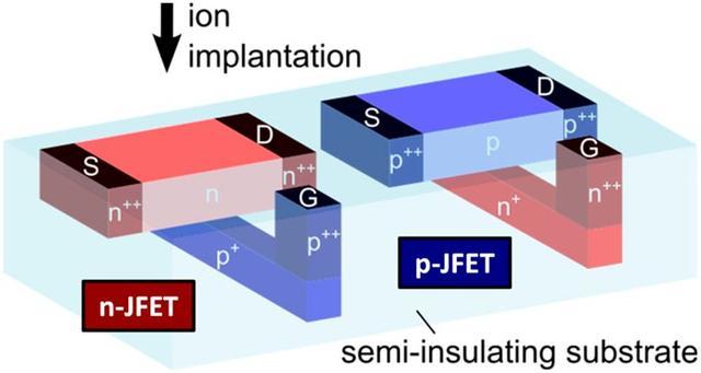
IT之家援引博文介绍,该晶体管采用商业芯片工厂普遍使用的“离子注入”(ion implantation)工艺打造,相关成果于 8 月 17 日发表在《APL Electronic Devices》。

研究团队选择“结型场效应晶体管”(JFET)结构,并将栅极置于沟道下方,形成底栅(bottom-gate)布局。离子注入过程中,部分掺杂原子会沿晶体通道深入目标区域之外,形成“沟道效应”尾部。

传统顶栅结构难以补偿这一影响,导致设计阈值电压与实测值相差超过 2 V。底栅结构可捕获偏离预定深度的掺杂原子,让该偏差在 400℃ 下缩小至 0.1 V 以内。

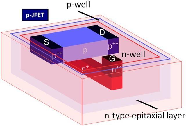
该科研团队为了减少高温漏电,团队还加入“双阱”(double-well)隔离结构。该结构通过 pn 结隔离单个器件,避免依赖下方半绝缘碳化硅衬底。

Disclaimer: Investing carries risk. This is not financial advice. The above content should not be regarded as an offer, recommendation, or solicitation on acquiring or disposing of any financial products, any associated discussions, comments, or posts by author or other users should not be considered as such either. It is solely for general information purpose only, which does not consider your own investment objectives, financial situations or needs. TTM assumes no responsibility or warranty for the accuracy and completeness of the information, investors should do their own research and may seek professional advice before investing.
Most Discussed

  1. 1


  2. 2


  3. 3


  4. 4


  5. 5


  6. 6


  7. 7


  8. 8


  9. 9


  10. 10